
Author Affiliations
Abstract
1 Center for Nanoscale Characterization & Devices, Wuhan National Laboratory for Optoelectronics, Huazhong University of Science and Technology, Wuhan 430074, China
2 School of Physics and Technology, Center for Electron Microscopy, MOE Key Laboratory of Artificial Micro- and Nano-Structures, and the Institute for Advanced Studies, Wuhan University, Wuhan 430072, China
3 Ministry-of-Education Key Laboratory for the Green Preparation and Application of Functional Materials, Hubei Collaborative Innovation Center for Advanced Organic Chemical Materials, School of Materials Science and Engineering, Hubei University, Wuhan 430062, China
As the scaling down of semiconductor devices, it would be necessary to discover the structure-property relationship of semiconductor nanomaterials at nanometer scale. In this review, the quantitative characterization technique off-axis electron holography is introduced in details, followed by its applications in various semiconductor nanomaterials including group IV, compound and two-dimensional semiconductor nanostructures in static states as well as under various stimuli. The advantages and disadvantages of off-axis electron holography in material analysis are discussed, the challenges facing in-situ electron holographic study of semiconductor devices at working conditions are presented, and all the possible influencing factors need to be considered to achieve the final goal of fulfilling quantitative characterization of the structure-property relationship of semiconductor devices at their working conditions.
Journal of Semiconductors
2022, 43(4): 041103
Author Affiliations
Abstract
1 Hubei Key Laboratory of Intelligent Wireless Communications, College of Electronics and Information Engineering, South-central University for Nationalities, Wuhan, Hubei 430074, China
2 Wuhan National Laboratory for Optoelectronics (WNLO), School of Physics, Huazhong University of Science and Technology, Wuhan, Hubei 430074, China
Wepresent a novel method for engineering ultra-flattened-dispersion photonic crystal fibers with uniform air holes by rotations of inner air-hole rings around the fiber core. By choosing suitable rotation angles of each inner ring, theoretical results show that normal, anomalous, and nearly zero ultra-flattened-dispersion fibers in wide spectra ranges of interest can be obtained alternatively. Moreover, in our dispersion sensitive analysis, these types of fibers are robust to variations from optimal design parameters. The method is suitable for the accurate adjustment of fiber dispersion within a small range, which would be valuable for the fabrication of ultra-flattened-dispersion fibers and also have potential applications in wide-band high-speed optical communication systems.
Photonic crystal fibers Fiber properties Fiber design and fabrication Photonics Research
2014, 2(2): 02000059
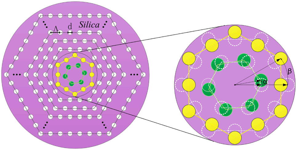
Author Affiliations
Abstract
In this study, we propose that by diminishing only the pitch of the innermost air-holes-ring of a HF1 photonic crystal fiber, both an effective mode area up to 100 μm2 at 1.55 μm wavelength and nearly zero dispersion of 0.2 ± 1 ps/(km·nm) within a spectrum range of 1.23–1.65 μm can be achieved simultaneously. Because only one parameter is needed to be tuned in the proposed design scheme, the fiber would be easier to be fabricated compared to other fibers using either multiple changing parameters or additional kinds of materials and would have potential applications in optical communications.
060.5295 Photonic crystal fibers 060.2270 Fiber characterization 060.2430 Fibers, single-mode 060.2280 Fiber design and fabrication Chinese Optics Letters
2014, 12(s1): S10607


